Types of Optical Lasers and Photo diode
What is TOSA and ROSA?
TOSA is responsible for converting electrical signals into optical signals. It acts as the transmitting component in an optical communication system.
The laser diode generates the optical signal by converting electrical input into light. Common types include Distributed Feedback lasers and Vertical Cavity Surface Emitting Lasers then the modulator is used to modulate the light generated by the laser diode to encode data onto the optical signal. Lens are used to focus the light into the optical fibre, ensuring efficient coupling of the optical signal into the fibre.
ROSA is responsible for converting optical signals back into electrical signals. It acts as the receiving component in an optical communication system. The photodiode detects the incoming optical signal and converts it into an electrical current common types include PIN photodiodes and Avalanche Photodiodes .The weak electrical signal generated by the photodiode is amplified to a level suitable for further processing by the receiver electronics. Filters are used to select the desired wavelength and reduce noise.
1. Fabry-Perot (FP) Laser Diode:
The Fabry-Perot resonator cavity. The mirror facets are constructed by making two parallel clefts along natural cleavage planes of the semiconductor crystal. The purpose of the mirrors is to establish a strong optical feedback in the longitudinal direction. This feedback mechanism converts the device into an oscillator (and hence a light emitter) with a gain mechanism that compensates for optical losses in the cavity at certain resonant optical frequencies. The sides of the cavity are simply formed by roughing the edges of the device to reduce unwanted emissions in the lateral directions.
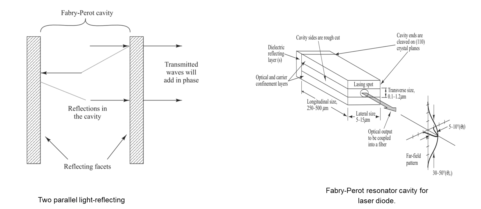
As the light reflects back and forth within the Fabry-Perot cavity, the electric fields of the light interfere on successive round trips. Those wavelengths that are integer multiples of the cavity length interfere constructively so that their amplitudes add when they exit the device through the right-hand facet. All other wavelengths interfere destructively and thus cancel themselves out. The optical frequencies at which constructive interference occurs are the resonant frequencies of the cavity. Consequently, spontaneously emitted photons that have wavelengths at these resonant frequencies reinforce themselves after multiple trips through the cavity so that their optical field becomes very strong. The resonant wavelengths are called the longitudinal modes of the cavity because they resonate along the length of the
cavity.
Applications:
- SFP Transceivers (1G Ethernet):
FP laser diodes are commonly used in SFP transceivers for 1 Gigabit Ethernet (1G) applications.
These transceivers are typically used in short-distance communication scenarios within data centres, enterprise networks, and Fibre-to-the-Home (FTTH) deployments.
- SFP+ Transceivers (10G Ethernet):
While SFP+ transceivers can use more advanced laser types like DFB, FP lasers may still be used in certain cost-sensitive applications or for compatibility with existing infrastructure.
Uses:
FP laser diodes are chosen for their cost-effectiveness, reliability, and suitability for applications where moderate data rates and shorter transmission distances are sufficient.
FP lasers can operate at various wavelengths, the most commonly used wavelengths are 850 nm for multimode fibre applications and 1310 nm and 1550 nm for single-mode and long-haul applications
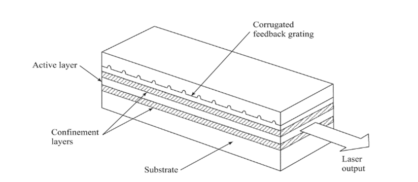
2. Distributed-feedback (DFB) laser diode:
An elegant approach to single-frequency operation which has found widespread application involves the use of distributed resonators, fabricated into the laser structure to give integrated wavelength selectivity. The structure which is employed is the distributed Bragg diffraction grating which provides periodic variation in refractive index in the laser heterostructure waveguide along the direction of wave propagation so that feedback of optical energy is obtained through Bragg reflection rather than by the usual cleaved mirrors.
Applications (The above fig is the proof of all this application)
- Long distance communication
Single-mode fibre systems, especially those covering long distances, require the narrow linewidth and high stability of DFB lasers to minimise dispersion and maintain signal integrity.
- High Data Rates:
DFB lasers can support high data rates with low noise, essential for modern high-speed optical networks like 10G, 25G, 40G, 100G, 200G, 400G, and beyond.
- Wavelength Division Multiplexing (WDM) Systems:
In DWDM systems, where channels are closely spaced, the precise wavelength control of DFB lasers prevents crosstalk and interference, ensuring reliable communication.
- Stable Wavelength Requirements:
Applications that require stable wavelengths over varying temperatures and operating conditions benefit from the intrinsic stability of DFB lasers.
Uses:
DFB lasers are integral to high-performance optical transceivers, especially in applications demanding high data rates, long-distance transmission, and wavelength stability. They are preferred in transceivers like SFP+, QSFP+, QSFP28, QSFP56, QSFP-DD, and QSFP112
3. Vertical-Cavity Surface-Emitting Lasers (VCSELs)
The special feature of a vertical-cavity surface-emitting laser is that the light emission is perpendicular to the semiconductor surface, as shown in Fig This feature facilitates the integration of multiple lasers into a single chip in one-or two-dimensional arrays, which makes them attractive for wavelength-division-multiplexing applications.VCSEL use Distributed Bragg Reflectors (DBRs) as mirrors to provide high reflectivity.These mirrors are essential for the vertical lasing process
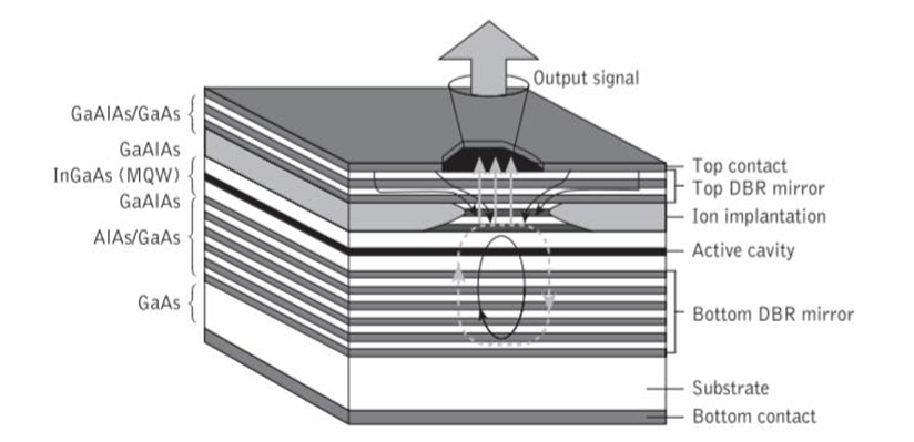
VCSELs are advantageous due to their cost-effective manufacturing process. They are easier and cheaper to produce in large arrays compared to edge-emitting lasers. Additionally, VCSELs can be tested on-wafer before being cut and packaged, which reduces manufacturing costs and ensures higher yields. These lasers are typically more energy-efficient, making them suitable for high-density, low-power applications. Their efficiency is particularly beneficial for battery-operated devices and systems requiring minimal power consumption. Moreover, VCSELs emit a circular beam that is easier to couple into optical fibres and other components, enhancing coupling efficiency and reducing alignment issues. Furthermore, VCSELs exhibit better temperature stability than many other types of lasers, ensuring consistent performance over a wide range of operating conditions and making them reliable for various applications
Applications
- Short-Range Optical Communication:
VCSELs are commonly used for data communication over short distances (typically up to 300 metres) using multimode fibre.
- Data Centers:
Their low cost and high efficiency make them ideal for short-reach connections.
Uses:
VCSELs are a versatile and cost-effective choice for a variety of applications, particularly where short-distance optical communication and high efficiency are essential.In optical transceivers like SFP,SFP+,QSFP,QSFP+,QSFP28.
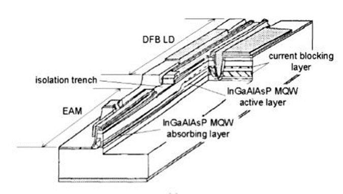
4. Electro-absorption modulator integrated lasers (EMLs)
Electro-absorption modulator integrated lasers (EMLs) are devices that combine a laser source with an electro-absorption modulator (EAM) in a single integrated chip. They are crucial components in high-speed optical communication systems, offering benefits in terms of compactness, performance, and power efficiency. Typically, the laser section uses a semiconductor gain medium like InGaAsP or InP.Many EMLs utilise a DFB laser for single-mode operation, providing a stable and narrow linewidth laser output. The laser is electrically pumped to achieve population inversion and stimulated emission.The EAM operates based on the Franz-Keldysh effect or the Quantum Confined Stark Effect (QCSE). Applying a voltage to the EAM changes the absorption coefficient, modulating the light passing through. EAMs often use quantum wells in the same material system as the laser The laser generates continuous-wave (CW) light, which is directed into the EAM. By applying a varying electric field to the EAM, the absorption properties are modulated, effectively modulating the intensity of the light. This converts the CW laser output into a modulated signal suitable for optical communication.
Photodiodes:
At the output end of an optical transmission line, there must be a receiving device that interprets the information contained in the optical signal. The first element of this receiver is a photodetector. Thephotodetector senses the luminescent powder falling upon it and converts the variation of this optical power into a correspondingly varying electric current. Since the optical signal is generally weakened and distorted when it emerges from the end of the fibre, the photodetector must meet very high performance requirements.
Pin Photodiode:
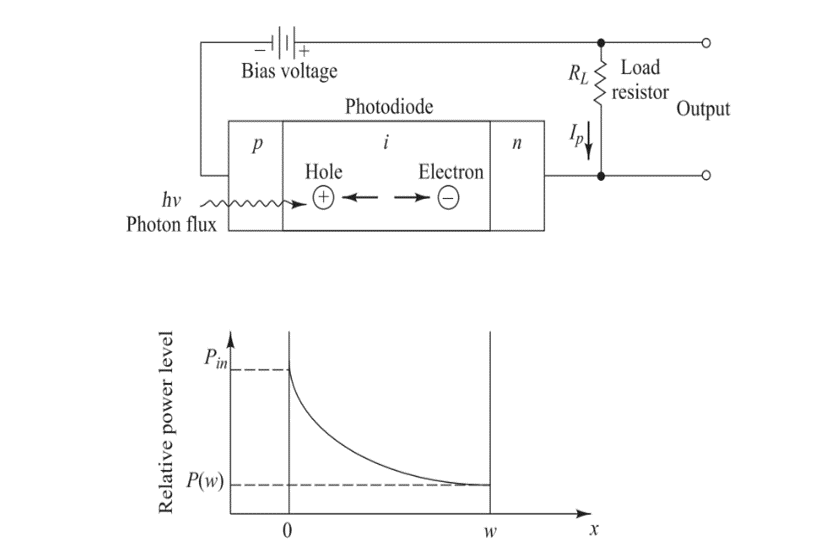
The most common semiconductor photodetector is the pin photodiode, shown schematically in The device structure consists of p and n regions separated by a very lightly n-doped intrinsic region. In normal operation a sufficiently large reverse-bias voltage is applied across the device so that the intrinsic region is fully depleted of carriers. That is, the intrinsic n and p carrier concentrations are negligibly small in comparison with the impurity concentration in this region. When an incident photon has an energy greater than or equal to the bandgap energy of the semiconductor material, the photon can give up its energy and excite an electron from the valence band to the conduction band. This absorption process generates mobile electron–hole pairs These electrons and holes are known as photocarriers, since they are photon-generated charge carriers that are available to produce a current flow when a bias voltage is applied across the device. The number of charge carriers is controlled by the concentration level of impurity elements that are intentionally added to the material
The photodetector is normally designed so that these carriers are generated mainly in the depletion region (the depleted intrinsic region) where most of the incident light is absorbed. The high electric field present in the depletion region causes the carriers to separate and be collected across the reverse-bias junction. This gives rise to a current flow in an external circuit, with one electron flowing for every carrier pair generated. This current flow is known as the photocurrent.
Representation of a pin photodiode circuit with an applied reverse bias. An incident optical power level decays exponentially inside the device.
Application
- Optical Communication:
Converting optical signals to electrical signals in fibre optic communication systems. High sensitivity and fast response time make PIN photodiodes ideal for detecting light pulses in high-speed data transmission.
- Optical Power Monitoring:
Monitoring optical power levels in fibre optic networks. PIN photodiodes can measure the intensity of light, helping to ensure that the optical power levels are within the desired range.
- Optical Sensing:
Used in various sensors for measuring light intensity, presence, and other optical properties.The broad wavelength range and high sensitivity allow PIN photodiodes to detect various light signals accurately.
Uses:
In optical transceivers, they are critical for converting optical signals to electrical signals, ensuring high-speed data transmission and accurate signal detection in systems ranging from SFP to QSFP-DD for small to medium range.
Avalanche Photodiode
Avalanche photodiodes (APDs) internally multiply the primary signal photocurrent before it enters the input circuitry of the following amplifier. This increases receiver sensitivity, since the photocurrent is multiplied before encountering the thermal noise associated with the receiver circuit. In order for carrier multiplication to take place, the photogenerated carriers must traverse a region where a very high electric field is present. In this high-field region, a photogenerated electron or hole can gain enough energy so that it ionises bound electrons in the valence band upon colliding with them. This carrier multiplication mechanism is known as impact ionisation. The newly created carriers are also accelerated by the high electric field, thus gaining enough energy to cause further impact ionization. This phenomenon is the avalanche effect. Below the diode breakdown voltage a finite total number of carriers are created, whereas above breakdown the number can be infinite. A commonly used structure for achieving carrier multiplication with very little excess noise is the reach-through construction in Fig The reach-through avalanche photodiode (RAPD) is composed of a high-resistivity p-type material deposited as an epitaxial layer on a p+ (heavily doped p-type) substrate. A p-type diffusion or ion implant is then made in the high-resistivity material, followed by the construction of an n+ (heavily doped n-type) layer. For silicon, the dopants used to form these layers are normally boron and phosphorus, respectively. This configuration is referred to as p+ p pn+ reach-through structure. The p layer is basically an intrinsic material that inadvertently has some p doping because of imperfect purification.
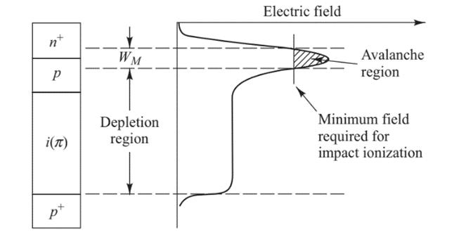
The term “reach-through” arises from the photodiode operation. When a low reverse-bias voltage is applied, most of the potential drop is across the pn+ junction. The depletion layer widens with increasing bias until a certain voltage is reached at which the peak electric field at the pn+ junction is about 5–10 percent below that needed to cause avalanche breakdown. At this point, the depletion layer just“reaches through” to the nearly intrinsic p region.
Applications
- Long-Distance Communication:
The high sensitivity of APDs allows for the detection of weak signals over long distances, reducing the need for repeaters.
- High-Speed Communication: APDs can handle high data rates while providing the necessary sensitivity for reliable signal detection.
Uses:
Avalanche Photodiodes (APDs) are crucial in optical transceivers for applications requiring high sensitivity, such as long-distance and high-speed communication. Their internal gain mechanism allows for the detection of weak signals, making them ideal for use in transceivers ranging from SFP to QSFP-DD.
Summary:
Parameter | Fabry-Pérot (FP) Laser | Distributed Feedback (DFB) Laser | Vertical-Cavity Surface-Emitting Laser (VCSEL) | Electro-absorption modulator integrated lasers |
Construction | Two parallel mirrors at the ends of the semiconductor material | Grating structure within the semiconductor material | Distributed Bragg Reflectors (DBRs) on both sides of the active region | Combines a laser source and an electro-absorption modulator on a single chip |
Principle | Multimode operation with multiple longitudinal modes | Single-mode operation with a narrow linewidth | Multimode operation with a circular beam profile | The laser generates continuous-wave (CW) light |
Stability | Moderate | High | Moderate | High |
O/p Power | Moderate | High | Moderate | High |
According to distance applicable | Short to medium distances | Medium to long Distances LR-400G QSFP-DD 200G QSFP56 100G QSFP28 40G QSFP+ 25G SFP28 10G SFP+ | Very Short distances, typically within data centres SR- 800G QSFP-DD 400G QSFP-DD 200G-QSFP56 100G QSFP28 40G QSFP+ 25G SFP28 10G SFP+ | Long-distance communication, often exceeding 10 km and up to 80 km ER-100G QSFP28 |
Optical lasers and photodiodes are critical components in fiber optic communication systems, each serving distinct roles and applications. FP lasers and VCSELs are suited for short-distance communication due to their cost-effectiveness and ease of integration. In contrast, DFB and tunable lasers are essential for long-distance and flexible wavelength applications, respectively. On the detection side, PIN photodiodes are used for LR,FR range , while APDs provide enhanced sensitivity for long-distance and high-speed communication(ZR and ER). The choice of laser and photodiode type significantly impacts the performance and suitability of a fiber optic communication system for specific applications.